Samsung’s Yield Crisis Is TSMC’s Windfall
Chip manufacturing is a business where fractions of a percentage point determine winners and losers. Yield rate – the share of functional chips produced from a single wafer – dictates cost, delivery timelines, and ultimately which company secures the next big contract. Samsung’s foundry division has been fighting a visible and costly battle with yield problems on its most advanced nodes, and that struggle is handing TSMC a widening competitive edge at exactly the moment when AI-driven chip demand is accelerating across the industry.
The timing could not be worse for Samsung. Major chip designers who once split orders between the two foundries as a hedging strategy are increasingly consolidating their most critical work with TSMC. When a company cannot trust that a sufficiently high percentage of its ordered chips will actually work, the calculus shifts fast – and right now, that calculus is shifting hard against Samsung.
What Yield Problems Actually Mean in Practice
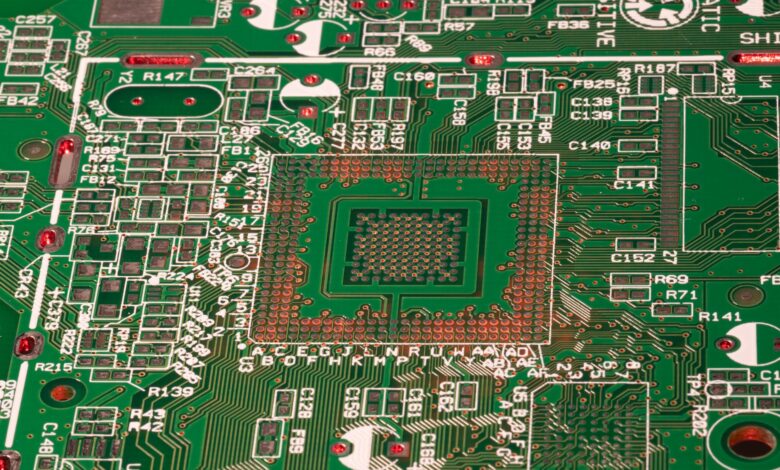
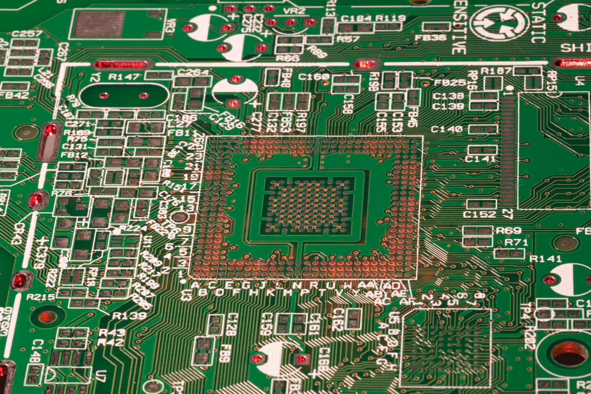
A foundry’s yield rate is rarely disclosed publicly, but its effects are visible everywhere. When yields are low, the cost per functioning chip rises because the same amount of silicon, energy, and labor produces fewer usable units. That cost gets passed down the chain. A chip designer paying for wafers with poor yields either absorbs the extra cost or passes it to customers – neither option is attractive when a competitor’s foundry is producing at significantly higher efficiency.
Samsung’s difficulties have been most acute on its 3nm Gate-All-Around (GAA) process node, which the company was first to bring to market. Being first, however, has not translated into being better. The GAA architecture requires extraordinarily precise manufacturing conditions, and Samsung’s process has struggled to hit the yield thresholds that would make it economically viable for high-volume production. Fabless chip companies designing at the cutting edge need confidence in mass production economics – not just a proof-of-concept that the node technically works.

TSMC’s Structural Advantage Deepens
TSMC’s 3nm node, built on a more conservative FinFET architecture, has reportedly achieved considerably more stable yields than Samsung’s GAA equivalent. That consistency is what fills order books. Nvidia, Apple, AMD, and Qualcomm – companies whose product cycles depend on predictable chip volumes – have maintained or deepened their commitment to TSMC as Samsung’s issues have persisted. The pattern shows how reputation and operational reliability compound over time in this industry.
There is also a talent and process knowledge dimension that rarely gets discussed. TSMC has spent decades building proprietary process libraries, equipment calibration expertise, and a workforce deeply specialized in high-volume precision manufacturing. That institutional knowledge is not something a competitor replicates in a short period, even with aggressive capital investment. Samsung’s foundry arm is competing against not just TSMC’s current factories but the accumulated process refinement of thirty-plus years of focused production.
Samsung has invested heavily in its foundry ambitions, announcing capacity expansions in South Korea and a major fabrication facility in Taylor, Texas. But capital expenditure alone does not solve a yield problem rooted in process chemistry and equipment calibration. The Texas plant, still under construction, is years away from operating at meaningful volume – and the question of whether Samsung can resolve its yield issues before TSMC further consolidates its customer base is an open one.
The broader export control environment adds another layer of complexity for the industry. As ASML’s export restrictions tighten and the gap between Western and Chinese chipmakers widens, the pressure on non-TSMC foundries to offer a credible alternative intensifies – because customers want supply chain diversification but cannot afford to sacrifice yield reliability to get it.
What This Means for Chip Designers
For fabless semiconductor companies – those that design chips but own no factories – the Samsung yield situation is a sourcing headache. Diversifying foundry relationships is a standard risk management approach, but it only works if the secondary supplier can actually deliver. Right now, Samsung’s foundry cannot serve as a full backup for leading-edge nodes in the way chip designers would need, which leaves the industry more concentrated around TSMC than most companies would prefer.
Some chip designers have begun exploring what a future split might look like: using TSMC for the most performance-sensitive, yield-critical components while routing less demanding production to Samsung or other foundries. This kind of segmented sourcing works for larger companies with the engineering bandwidth to manage multiple supply relationships, but smaller fabless firms simply default to TSMC and absorb the pricing premium rather than take on execution risk.
Samsung’s Path Forward Is Narrow
Samsung’s foundry leadership has publicly acknowledged yield challenges and signaled process improvements in development. The company is not standing still – its engineers are iterating on the GAA architecture, and there is genuine technical progress happening. But the semiconductor industry moves on customer timelines, not R&D timelines. A chip designer planning a new product family needs foundry commitments 18 to 24 months before volume production. If Samsung cannot demonstrate yield stability in that window, the design wins go elsewhere, and redesigning for a different foundry is expensive and time-consuming enough that most companies will not reverse course even if Samsung catches up later.
There is also a psychological dynamic at work in the foundry market. Reputation for yield consistency is nearly impossible to rebuild quickly once it is damaged. TSMC cultivated its position over years of reliability, and Samsung will need an extended track record of stable, high-yield production at advanced nodes before major customers allocate their most critical work back to its fabs. The question for Samsung is whether it can generate that track record before AI-era chip demand patterns lock in a supply chain architecture where TSMC’s dominance simply becomes the default assumption rather than the considered choice.
For TSMC, every quarter that Samsung’s yield problems persist translates into pricing power, customer loyalty, and the ability to attract the most ambitious chip designs – including next-generation AI accelerators where the economic stakes are highest. A single AI chip program generating tens of billions in annual wafer revenue represents the kind of contract that reshapes a foundry’s financials for years. Samsung’s yield struggles do not just cost it today’s orders – they cost it the relationships that determine who gets the call when the next generation design cycle begins.