

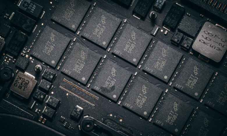
Samsung’s foundry division is losing ground to TSMC at a pace that is starting to look less like a temporary setback and more like a structural problem – one that major chip designers are quietly factoring into their long-term production decisions.
Where the Gap Is Actually Growing
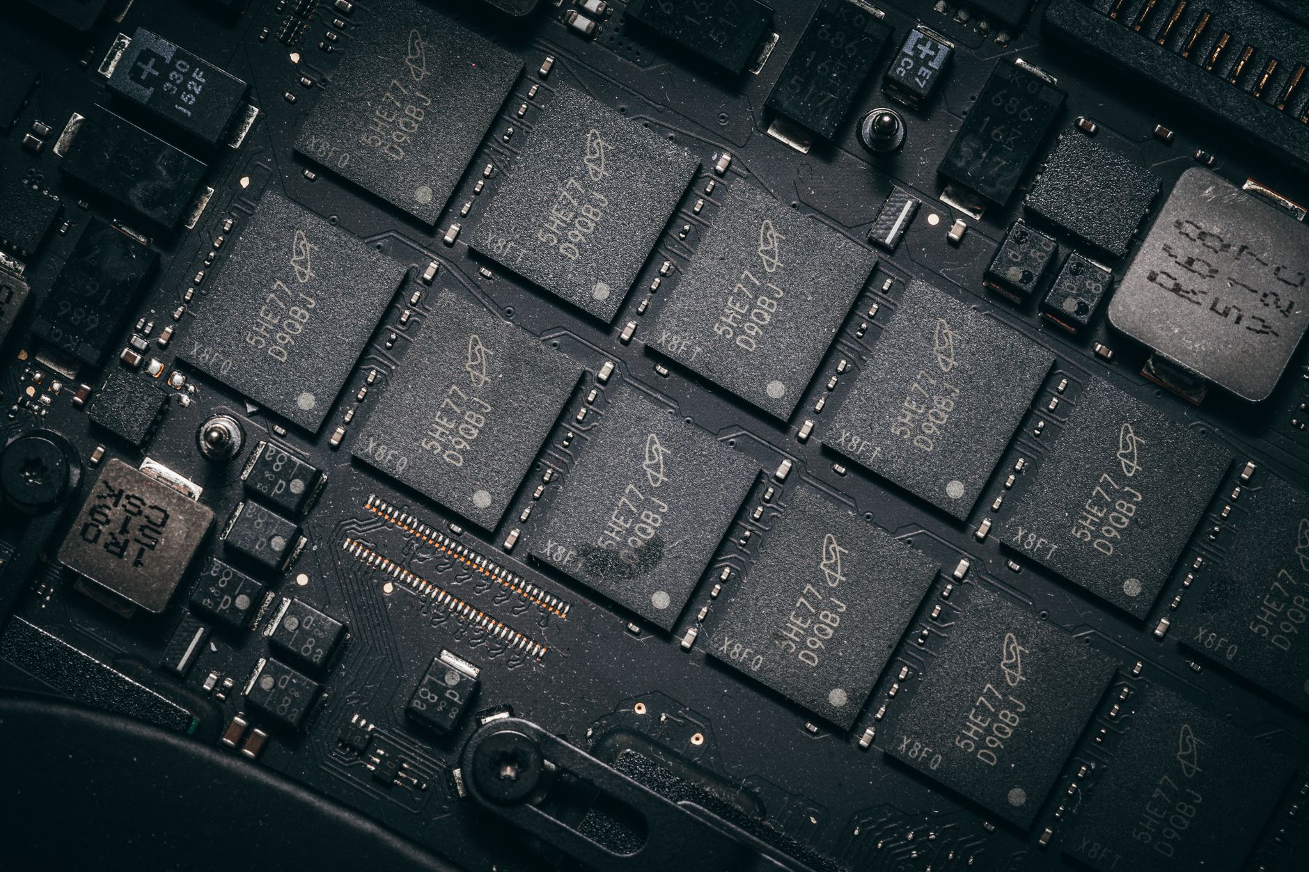
The core issue is yield rates. TSMC has spent years refining its 3nm and now 2nm processes to the point where chips come off the production line with far fewer defects per wafer. Samsung’s equivalent nodes have struggled to match that consistency, and for companies designing high-end processors – where a single chip can cost hundreds of dollars in silicon alone – defect rates are not a minor inconvenience. They are a direct hit to profitability and delivery schedules.
Apple, Qualcomm, and Nvidia have all deepened their reliance on TSMC for their most advanced silicon. That is not a coincidence. Each of those companies went through its own evaluation of what Samsung’s foundry could offer and, for cutting-edge work, concluded TSMC was the safer bet. Samsung still manufactures chips – including some of its own Exynos processors and certain mid-range mobile silicon – but the flagship design wins that validate a foundry’s prestige keep gravitating toward TSMC’s fabs in Taiwan and increasingly in Arizona.
Samsung has acknowledged the yield problems internally, and the company has publicly committed billions to fix them. Its 3nm gate-all-around transistor architecture was supposed to be a leapfrog moment – a technology that Samsung adopted before TSMC. The manufacturing reality did not match the architectural ambition. Customers who evaluated the node found the yields too unpredictable for mass production at scale, and the early momentum Samsung hoped to build never materialized into significant design wins from external customers.
TSMC, meanwhile, has been methodically improving its own gate-all-around process – called nanosheet technology – for its 2nm node, which is scheduled to enter risk production. The company’s reputation for hitting yield targets on schedule has become self-reinforcing: chip designers plan their roadmaps around TSMC’s timelines because those timelines have historically been reliable. That reliability is itself a competitive advantage that no single process generation can undo quickly.
Why This Is Harder to Fix Than It Looks
Samsung’s foundry challenges are not simply a matter of investing more capital. The company spends heavily on semiconductor manufacturing – it is one of the largest capital expenditure programs in the technology industry. The problem is that advanced chip manufacturing requires not just equipment and money but an accumulated base of process knowledge that takes years to develop. TSMC has been running high-volume advanced nodes for longer, and that operating history translates into finely tuned recipes for photolithography, etch, and deposition steps that competitors cannot replicate overnight.
There is also an organizational dimension. Samsung operates as both a chip designer and a foundry, which creates an inherent tension. External customers worry – sometimes openly – that Samsung’s foundry business has less incentive to protect their intellectual property and process secrets when Samsung’s own design teams are competing in the same chip markets. TSMC’s entire business model is built on being a pure-play foundry with no competing chip design division. That structural neutrality is something TSMC markets aggressively, and it resonates with customers who are handing over their most sensitive design files.
The talent dynamic compounds the difficulty. TSMC has cultivated deep institutional knowledge in its engineering workforce, and many of the process engineers with the most relevant experience in advanced nodes have spent their careers there. Samsung has made efforts to build its own engineering bench, but the gap in process maturity means Samsung’s teams are still working through problems that TSMC’s engineers largely solved in prior process generations. This creates a lag that cannot be closed simply by hiring more people.
For customers evaluating foundry options, the calculus has become straightforward for the most demanding applications. Nvidia’s continued commitment to TSMC for its Blackwell architecture is a visible example of how the AI chip boom is consolidating around a single manufacturing partner rather than distributing across competing fabs. When a chip requires billions of transistors to function correctly at extreme speeds, yield rate differences of even a few percentage points between fabs become enormous cost and schedule variables.
Samsung is aware that its window to close the gap is not indefinite. TSMC’s 2nm node will likely lock in another generation of flagship customer relationships before Samsung’s yield improvements can catch up. Each generation where TSMC wins the premium design work gives TSMC additional revenue to fund the next node’s development, while Samsung’s foundry division gets less high-volume advanced work and thus fewer opportunities to refine its processes through production learning. The cycle compounds in TSMC’s favor.
What Samsung Is Actually Betting On
Samsung’s foundry strategy has shifted toward emphasizing its HBM memory integration capabilities and its presence in markets where TSMC is not the only viable option – including certain automotive, industrial, and legacy node segments where yield requirements are less extreme and relationships with Samsung’s broader electronics business carry weight. The company is also investing in its U.S. fab in Taylor, Texas, partly as a geopolitical hedge that positions it for government subsidy programs and supply-chain diversification efforts by American chip designers who want domestic options.

The Taylor fab investment is real, but it will not resolve the fundamental yield gap at the bleeding edge. What Samsung needs most – consistent, high-yield production at 3nm and below with a customer list that validates the capability – is exactly what keeps not materializing. Until a major external chip designer commits its highest-volume, most advanced product to Samsung’s foundry at scale, the credibility gap will persist, and competing for those design wins becomes harder the longer the gap holds.
Frequently Asked Questions
Why are chip designers choosing TSMC over Samsung’s foundry?
TSMC consistently delivers higher yield rates at advanced nodes, which directly reduces production costs and schedule risk for high-end chip designers.
Can Samsung close the gap with TSMC in advanced chip manufacturing?
Samsung is investing heavily in its foundry business, but closing the yield and process maturity gap requires years of high-volume production learning that cannot be accelerated easily.